Description of the processes for the Production of Silicon and Thin film Solar cells and their applications
Production of Silicon and Thin film Solar cells and their applications – This article contains full details on the production of Silicon and Thin Film Solar Cells. Definitions of Silicon and Thin Film Solar Cells, History of Silicon and Thin Film Solar Cells, processes involved in the production of Silicon and Thin Film Solar cells, Applications of Silicon and Thin Film Solar Cells, Advantages and Disadvantages of Silicon and Thin Film Solar Cells.
Contents
INTRODUCTION
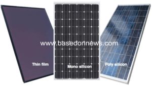
A thin-film solar cell is a second generation solar cell that is made by depositing one or more thin layers, or thin film (TF) of photovoltaic material on a substrate, such as glass, plastic or metal. Thin-film solar cells are commercially used in several technologies, including cadmium telluride (CdTe), copper indium gallium diselenide (CIGS), and amorphous thin-film silicon (a-Si, TF-Si).
Film thickness varies from a few nanometers (nm) to tens of micrometers (µm), much thinner than thin-film’s rival technology, the conventional, first-generation crystalline silicon solar cell (c-Si), that uses wafers of up to 200 µm. This allows thin film cells to be flexible, and lower in weight. It is used in building integrated photovoltaics and as semi-transparent, photovoltaic glazing material that can be laminated onto windows. Other commercial applications use rigid thin film solar panels (sandwiched between two panes of glass) in some of the world’s largest photovoltaic power stations.
Thin-film technology has always been cheaper but less efficient than conventional c-Si technology. However, it has significantly improved over the years. The lab cell efficiency for CdTe and CIGS is now beyond 21 percent, outperforming multicrystalline silicon, the dominant material currently used in most solar PV systems. Accelerated life testing of thin film modules under laboratory conditions measured a somewhat faster degradation compared to conventional PV, while a lifetime of 20 years or more is generally expected. Despite these enhancements, market-share of thin-film never reached more than 20 percent in the last two decades and has been declining in recent years to about 9 percent of worldwide photovoltaic installations in 2013.
Other thin-film technologies that are still in an early stage of ongoing research or with limited commercial availability are often classified as emerging or third generation photovoltaic cells and include organic, dye-sensitized, and polymer solar cells, as well as quantum dot, copper zinc tin sulfide, nanocrystal, micromorph, and perovskite solar cells.
Photovoltaics (PV) is a term which covers the conversion of light into electricity using semiconducting materials that exhibit the photovoltaic effect, a phenomenon studied in physics, photochemistry, and electrochemistry.
A typical photovoltaic system employs solar panels, each comprising a number of solar cells, which generate electrical power. PV installations may be ground-mounted, rooftop mounted or wall mounted. The mount may be fixed, or use a solar tracker to follow the sun across the sky.
Solar PV has specific advantages as an energy source: once installed, its operation generates no pollution and no greenhouse gas emissions, it shows simple scalability in respect of power needs and silicon has large availability in the Earth’s crust
Silicon is a chemical element with symbol Si and atomic number 14. It is a hard and brittle crystalline solid with a blue-grey metallic lustre; and it is a tetravalent metalloid and semiconductor. It is a member of group 14 in the periodic table: carbon is above it; and germanium, tin, and lead are below it. It is relatively unreactive. Because of its large chemical affinity for oxygen, it was not until 1823 that Jöns Jakob Berzelius was first able to prepare it and characterize it in pure form. Its melting and boiling points of 1414 °C and 3265 °C respectively are the second-highest among all the metalloids and nonmetals, being only surpassed by boron. Silicon is the eighth most common element in the universe by mass, but very rarely occurs as the pure element in the Earth’s crust. It is most widely distributed in dusts, sands, planetoids, and planets as various forms of silicon dioxide (silica) or silicates. Over 90% of the Earth’s crust is composed of silicate minerals, making silicon the second most abundant element in the Earth’s crust (about 28% by mass) after oxygen.
Most silicon is used commercially without being separated, and often with little processing of the natural minerals. Such use includes industrial construction with clays, silica sand, and stone. Silicates are used in Portland cement for mortar and stucco, and mixed with silica sand and gravel to make concrete for walkways, foundations, and roads. They are also used in whiteware ceramics such as porcelain, and in traditional quartz-based soda-lime glass and many other specialty glasses. Silicon compounds such as silicon carbide are used as abrasives and components of high-strength ceramics. Silicon is the basis of the widely used synthetic polymers called silicones.
Elemental silicon also has a large impact on the modern world economy. Most free silicon is used in the steel refining, aluminium-casting, and fine chemical industries (often to make fumed silica). Even more visibly, the relatively small portion of very highly purified elemental silicon used in semiconductor electronics (< 10%) is essential to integrated circuits — most computers, cell phones, and modern technology depend on it.
Silicon is an essential element in biology, although only traces are required by animals. However, various sea sponges and microorganisms, such as diatoms and radiolaria, secrete skeletal structures made of silica. Silica is deposited in many plant tissues.
PROCESSES FOR THE PRODUCTION OF SILICON
Raw Materials
Silicon metal is made from the reaction of silica (silicon dioxide, SiO2) and carbon materials like coke, coal and wood chips. Silica is typically received in the form of metallurgical grade gravel. This gravel is 99.5% silica, and is 3 x 1 or 6 x 1 in (8 x 3 cm or 15 x 3 cm) in size. The coal is usually of low ash content (1-3% to minimize calcium, aluminum, and iron impurities), contains around 60% carbon, and is sized to match that of the gravel. Wood chips are usually hardwood of 1/2 x 1/8 inch size (1 x. 3 cm size). All materials are received as specified by the manufacturer.
The Manufacturing Process
The basic process heats silica and coke in a submerged electric arc furnace to high temperatures. High temperatures are required to produce a reaction where the oxygen is removed, leaving behind silicon. This is known as a reduction process. In this process, metal carbides usually form first at the lower temperatures. As silicon is formed, it displaces the carbon. Refining processes are used to improve purity.
The Reduction Process
- 1 The raw materials are weighed and then placed into the furnace through the top using the fume hood, buckets, or cars. A typical batch contains 1000 lb (453 kg) each of gravel and chips, and 550 lb (250 kg) of coal. The lid of the furnace, which contains electrodes, is placed into position. Electric current is passed through the electrodes to form an arc. The heat generated by this arc (a temperature of 4000° F or 2350 ° C) melts the material and results in the reaction of sand with carbon to form silicon and carbon monoxide. This process takes about six to eight hours. The furnace is continuously charged with the batches of raw materials.
- 2 While the metal is in the molten state, it is treated with oxygen and air to reduce the amount of calcium and aluminum impurities. Depending on the grade, silicon metal contains 98.5-99.99% silicon with trace amounts of iron, calcium and aluminum.
Cooling/Crushing
- 3 Oxidized material, called slag, is poured off into pots and cooled. The silicon metal is cooled in large cast iron trays about 8 ft (2.4 m) across and 8 in (20 cm) deep. After cooling, the metal is dumped from the mold into a truck, weighed and then dumped in the storage pile. Dumping the metal from the mold to the truck breaks it up sufficiently for storage. Before shipping, the metal is sized according to customer specifications, which may require a crushing process using jaw or cone crushers.
Packaging
- 4 Silicon metal is usually packaged in large sacks or wooden boxes weighing up to 3,000 lb (1,361 kg). In powder form, silicon is packaged in 50-lb (23-kg) plastic pails or paper bags, 500-lb (227-kg) steel drums or 3,000-lb (1,361-kg) large sacks or boxes.
Quality Control
Statistical process control is used to ensure quality. Computer-controlled systems are used to manage the overall process and evaluate statistical data. The two major process parameters that must be controlled are amounts of raw materials used and furnace temperatures. Laboratory testing is used to monitor the chemical composition of the final product and to research methods to improve the composition by adjusting the manufacturing process. Quality audits and regular assessments of suppliers also ensure that quality is maintained from extraction of raw materials through shipping of the final product.
Byproducts/Waste
With statistical process control, waste is kept to a minimum. A byproduct of the process, silica fume, is sold to the refractory and cement industries to improve strength of their products. Silica fume also is used for heat insulation, filler for rubber, polymers, grouts and other applications. The cooled slag is broken down into smaller pieces and sold to other companies for further processing. Some companies crush it into sandblasting material. Because electric arc furnaces emit particulate emissions, manufacturers must also comply with the Environmental Protection Agency’s (EPA) regulations.
Other methods for making silicon are being investigated, including supercooling liquid to form bulk amorphous silicon and a hydrothermal method for making porous silicon powder for optical applications.
APPLICATIONS OF THIN FILM SOLAR CELLS
1) Electronic powering circuits
2) Home light applications
3) Used in Solar fields
Advantages of Thin film Solar Cells
1) Easy to handle
2) More flexible than conventional solar cells
3) Available as thin wafer sheets
4) Cheaper than traditional panels
Disadvantages of Thin film Solar Cells
1) Less efficiency (20 to 30% of light converted into electricity)
2) Complex structure
3) Need to be very careful in handling
4) Can’t be used in astronomical devices.
APPLICATIONS OF SILICON
Silicon-based products comprise a versatile array of applications in the manufacturing industry. Because silicon is easily manipulated and tailored, with high temperature stability and age resistance, silicon often operates in conjunction with other materials to insulate, purify, soften, adhere, condition, or otherwise protect a product. Silicon-based materials are also used to improve appearance, transfer energy, and aid in reconstruction.
In applications where a product must adhere to another, silicon can enable bonding between the materials. On the other hand, in applications where a coating and an adhesive layer need to remain independent of one another, silicone can be tailored to inhibit adhesion, keeping each layer separate and preventing adhesion.
Because of the wide range of possible forms, silicon has extensive industrial applications. Silicone rubber is used effectively in computers and electronics, automobiles, textiles, healthcare products, construction and architecture, and household products—numerous materials we come in contact with on a daily basis, including even hair conditioner, depend on silicone or silicon-based polymers. Due to its exceptional insulation properties, silicone rubber in particular is used in the electrical industry to coat and protect wires.
Applications of Silicon-Based Products
- Computers and Electronics
Circuit boards in computers, cell phones, VCR and DVD players all depend on silicon-based materials, like hyper-pure polycrystalline, for protection and insulation. Silicone rubber is an essential component in providing proper insulation for computer and technical wiring—in the medical field, silicon products are quintessential in the composition of dialysis tubing, pacemaker leads, and lubricating needle syringes.
- Textiles and Household Products
When it comes to fabric, silicon can alter texture as well as make a material waterproof. Clothing protection from shrinking, stains, and wrinkles is also due in part to silicon-based materials, and even detergents, fabric softeners, and solvents depend on silicon to improve their capabilities. Personal products, like deodorant, antiperspirant, cosmetics, and moisturizers, obtain their smooth feel from silicon.
- Automobiles and Architecture
Not only does silicon protect material as delicate as clothing, it is also responsible for protecting buildings and cars from extreme weather and general environmental stress. Automobiles benefit from protective silicon-based coatings, sealants, and lubricants enabling optimum performance. From exterior car polish to interior airbag fabric coating, silicon products enhance numerous aspects of an automobile. Buildings, too, benefit from breathable coatings and waterproof exteriors that simultaneously allow trapped moisture to escape.
REFERENCES
Eranna, Golla (2014). Crystal Growth and Evaluation of Silicon for VLSI and ULSI. CRC Press. p. 7. ISBN 978-1-4822-3281-3.
Magnetic susceptibility of the elements and inorganic compounds, in Lide, D. R., ed. (2005). CRC Handbook of Chemistry and Physics (86th ed.). Boca Raton (FL): CRC Press. ISBN 0-8493-0486-5.
Ram, R. S.; et al. (1998). “Fourier Transform Emission Spectroscopy of the A2D–X2P Transition of SiH and SiD” (PDF). J. Mol. Spectr. 190: 341–352. PMID 9668026.
Terry, Mason L.; Straub, Axel; Inns, Daniel; Song, Dengyuan; Aberle, Armin G. (2005). “Large open-circuit voltage improvement by rapid thermal annealing of evaporated solid-phase-crystallized thin-film silicon solar cells on glass”. Applied Physics Letters. 86 (17): 172108. Bibcode:2005ApPhL..86q2108T. doi:10.1063/1.1921352.
Weast, Robert (1984). CRC, Handbook of Chemistry and Physics. Boca Raton, Florida: Chemical Rubber Company Publishing. pp. E110. ISBN 0-8493-0464-4.
LIKE our Facebook page for more updates.
Comment below if this is helpful and for questions and other things you need, comment below